Micron's G11 NAND: Doubling Density With Wafer Bonding
The memory maker plans to launch its next generation of 3D flash in late 2027, targeting 42 Gb/mm2 capacity and 5,400 MT/s speeds.
By Lorenzo Marshall ·
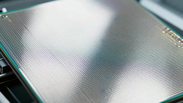
Micron Technology plans to begin production of its G11 3D NAND flash chips in the second half of 2027.
The new generation will double storage density to 42 Gb/mm2 in triple-level-cell format, up from the current 21 Gb/mm2 standard. This increase positions G11 above the next-generation products from competitors Kioxia and Samsung.
Performance metrics will also see substantial gains. Input/output speeds are projected to rise by 50 percent, reaching 5,400 MT/s from the current 3,600 MT/s. Additionally, the energy required to transfer each bit will drop by more than 25 percent.
The architectural shift relies on wafer-on-wafer bonding. This process allows Micron to manufacture the memory array and the peripheral logic on separate wafers. Each wafer uses a manufacturing process optimized for its specific function before the two are bonded together. While Micron has used CMOS-under-array designs for several years, this new bonding method offers greater flexibility in optimizing both the memory and logic components independently.
Scott DeBoer, Micron’s president and chief technology and products officer, stated that the company is introducing the technology now because it has become cost-effective and relevant to product specifications. He described G11 as the world's most advanced NAND based on this bonding approach. The chip will feature more than 400 layers, though the exact count of active wordlines has not been disclosed. The density improvement results from both additional layers and a smaller memory cell pitch.
The technology targets high-capacity solid-state drives for client and data center markets. It is also designed to support artificial intelligence workloads, which require higher bandwidth and lower power consumption. Micron intends to provide further technical details in 2027 as high-volume production approaches.
Beyond G11, the company aims to continue scaling in all three dimensions. DeBoer noted that future advancements will involve high-mobility materials and denser cell architectures. These changes are intended to improve transistor characteristics and reduce the energy needed to move data within the chips. Micron has not yet released specific targets or schedules for generations following G11.
Source: Tom's Hardware